I'm currently drafting a perfboard layout for this one. I'm confused about the "delay" pot. In the schematic, the pot's third pin is shown as going to the PT2399's pin #4 (DGND), which is directly connected to pin #3(AGND), which in turn is grounded. The path is shown as grey (the rest of gnd is green) in the pcb's layout. Wouldn't it be the same if the pot's third pin was grounded somewhere else?
Also, somewhere I can read more about how this specific part of the circuit (delay time) works, and also an overall analysis for this or similar PT2399 circuits?
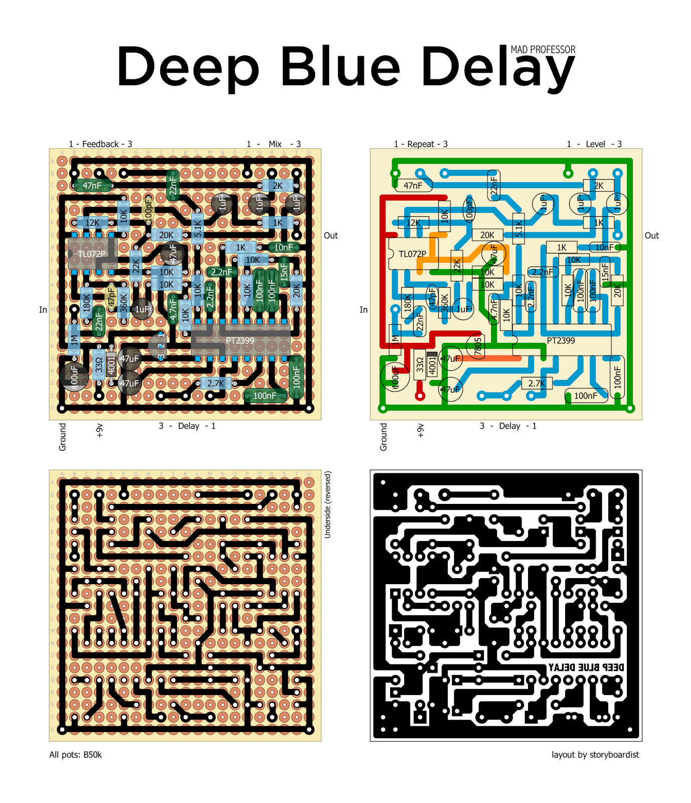
Link to schematics/pcb layout: http://www.tonepad.com/project.asp?id=51
Thanks for any help.
Question about Tonepad's Rebote 2.5
-
POTL

- Resistor Ronker
you need to connect the 4 pins to the first leg of the potentiometer delay
The third conclusion is connected to the ground
This is a typical mistake in the tonepad scheme, this site is quite outdated and many projects there have not been updated for a long time, surprised that someone else takes projects from there.
My advice is to look at the schematic diagrams and learn to breed boards yourself.
In addition to rebote delay (a long-obsolete project), many projects on the pt2399 chip including with an equalizer, tap tempo or chorus both separately from the delay and with it.
Alright, thanks, that makes sense. What you described is what's on the schematic. Now I'm just wondering if the boards they sell/sold worked at all, specially with things like the cap from the chip's 2nd pin being "grounded" to the trace from the pot to the 4th pin... But the schematic looks okay, I think I'll keep following it unless I find something else that's also simple with a relatively low parts count.
-
POTL
- Resistor Ronker
If you know how to make printed circuit boards, then pay attention to thisdiesel.riot wrote:Alright, thanks, that makes sense. What you described is what's on the schematic. Now I'm just wondering if the boards they sell/sold worked at all, specially with things like the cap from the chip's 2nd pin being "grounded" to the trace from the pot to the 4th pin... But the schematic looks okay, I think I'll keep following it unless I find something else that's also simple with a relatively low parts count.
or trace the card yourself on the computer